![[GMOS logo]](gmoslogo.gif)
| You are in: Instruments > GMOS > Performance and Use > GMOS Components > Detectors (North) |
|
GMOS-North Detectors |
The GMOS detector array consists of three 2048x4608 EEV chips arranged in a row. The table below gives a summary of the current detector/controller characteristics.
| Array | EEV | ||
| Pixel format | 6144x4608 pixels | ||
| Array layout | Three 2048x4068 chips in a row with ~0.5mm gaps | ||
| Pixel size | 13.5 microns square; 0.0727 arcsec/pixel | ||
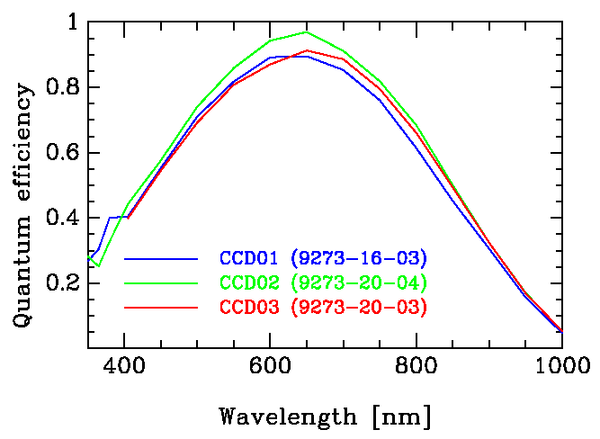
| Spectral Response | approx 0.3 to 0.9 microns [ data / plot ] | ||
| Bias level | Bias image | ||
| Flat field response | Fringe images Flat field images | ||
| Readout time | See observing overheads page | ||
| Chip | CCD 01 | CCD 02 | CCD 03 |
| Chip ref no. | EEV 9273-16-03 | EEV 9273-20-04 | EEV 9273-20-03 |
| Dark current* | 0.8 e-/pix/hr | 0.7 e-/pix/hr | 0.5 e-/pix/hr |
| Full Well ** | 150 ke- | 101 ke- | 159 ke- |
| Fringing at 900nm *** | 29% | 19% | 24% |
* Dark current measured at -120C by NOAO
** Saturation can be avoided by assuming 100ke- for all chips
*** (peak-valley)/mean, measured from images taken at NOAO
| Readout | Gain | Resulting average | |
| rate | level | Gain (e-/DN) | noise (e- rms) |
| Fast | High | 5.02 | 7.4 |
| " | Low | 2.49 | 4.9 |
| Slow | High | 4.40 | 4.8 |
| " | Low | 2.18 | 3.4 |
More information about the data format and GMOS data examples are available.
Binning: When pixel binning is used, the resulting datafile still contains overscan regions that are 32 samples wide.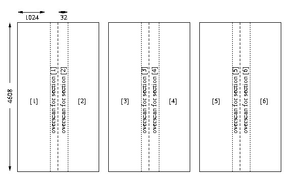
Layout of GMOS
detector array and structure of the output data file, when reading out
in 6-amp mode, with unbinned pixels.
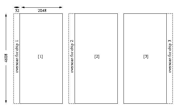
Layout of GMOS
detector array and structure of the output data file, when reading out
in 3-amp mode (using the 'best' three amps, R,R,L). Note the overscan
regions are not in the same place for each chip.
![]()
![]()
In original form: Isobel Hook
Last update: March 30, 2006; Kathy Roth